Error:
[DRC REQP-1712] Input clock driver: Unsupported PLLE2_ADV connectivity. The signal u_clk_wiz_0/inst/clk_in1 on the u_clk_wiz_0/inst/plle2_adv_inst/CLKIN1 pin of u_clk_wiz_0/inst/plle2_adv_inst with COMPENSATION mode ZHOLD must be driven by a clock capable IO.
[DRC REQP-1712] Input clock driver: Unsupported PLLE2_ADV connectivity. The signal u_clk_wiz_0/inst/clk_in1 on the u_clk_wiz_0/inst/plle2_adv_inst/CLKIN1 pin of u_clk_wiz_0/inst/plle2_adv_inst with COMPENSATION mode ZHOLD must be driven by a clock capable IO.
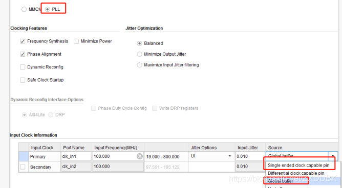
According to the prompt information, there should be a problem with the configuration of the clocking wizard.
Solution:
After selecting PLL, adjust the source from “single ended clock capable pin” to “global buffer”. No error will be reported when implementing again.